
Introduction
Solid-State Drives (SSDs) have fundamentally transformed data storage, replacing mechanical hard disk drives (HDDs) with semiconductor-based flash memory. Unlike HDDs that rely on spinning platters and moving read/write heads, SSDs store data in NAND flash memory cells—offering orders-of-magnitude improvements in speed, durability, and power efficiency. But beneath the sleek exterior of an M.2 stick or 2.5″ drive lies an extraordinarily complex system-on-chip (SoC) architecture that must solve some of the most challenging problems in computer engineering: translating host-friendly logical addresses into flash-friendly physical addresses, managing cells that wear out with every write, correcting inevitable bit errors, and orchestrating thousands of parallel operations across multiple NAND dies.
This article provides a comprehensive, end-to-end exploration of SSD architecture and the complete lifecycle of an I/O operation—from the moment your application issues a read() or write() system call to the nanosecond-level physics of charge trapping inside a NAND cell.
Part 1: SSD Internal Architecture
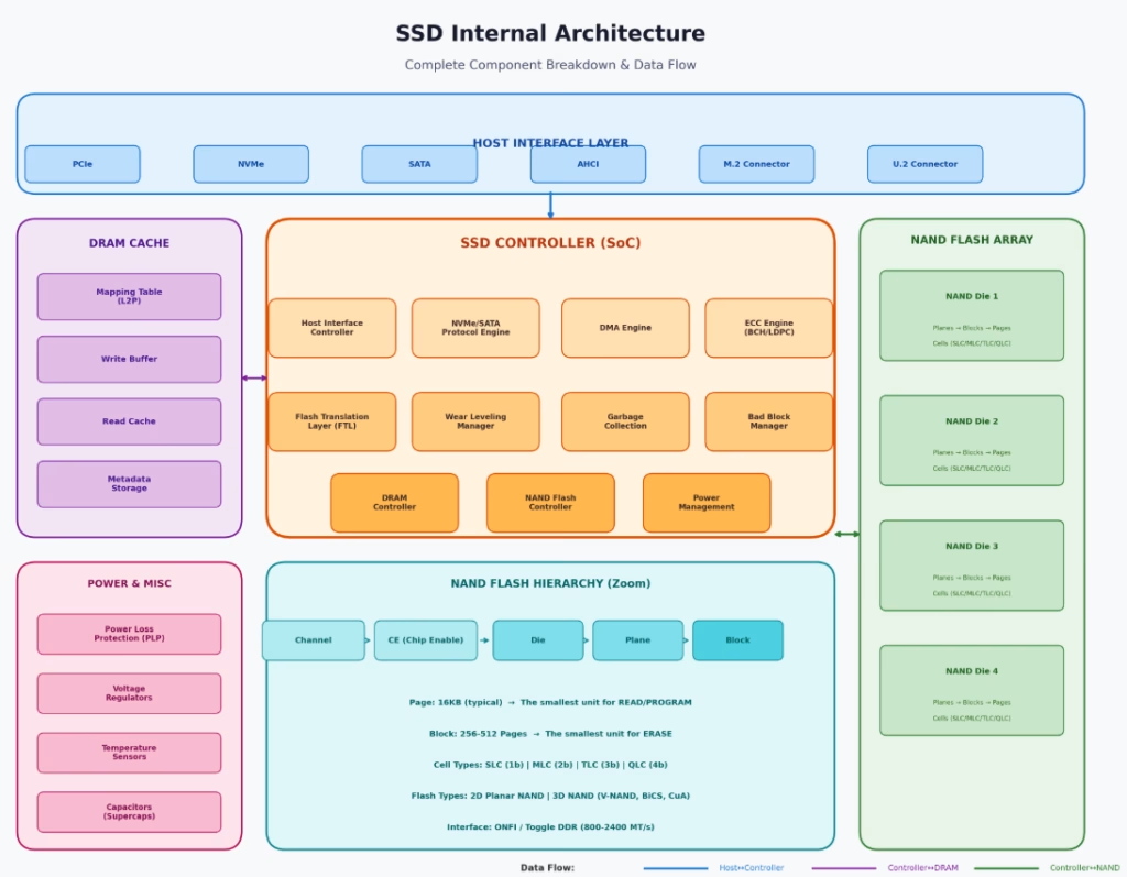
An SSD is not simply “flash memory with a connector.” It is a complete computer system with its own processor, memory, multiple specialized engines, and complex firmware. Let’s dissect every major component.
1.1 Host Interface Layer
The host interface is the SSD’s gateway to the outside world. Modern SSDs predominantly use:
- PCIe (Peripheral Component Interconnect Express): The physical electrical interface providing high-speed serial lanes. Consumer drives typically use x4 lanes, while enterprise drives may use x8.
- NVMe (Non-Volatile Memory Express): The protocol optimized for NAND flash, replacing the legacy AHCI protocol designed for spinning disks. NVMe supports up to 64K queues with 64K commands each, enabling massive parallelism.
- SATA/AHCI: Legacy interfaces still found in older systems, bottlenecked at ~550 MB/s due to the AHCI protocol’s single command queue design.
- Form Factors: M.2 (2280, 22110), U.2 (2.5″ enterprise), E1.S/E1.L (EDSFF for data centers), and PCIe add-in cards.
The Host Interface Controller inside the SSD manages the electrical signaling, link training, and protocol state machines.
1.2 SSD Controller (SoC)
The controller is the brain of the SSD—typically a multi-core ARM or proprietary RISC processor running at 500 MHz to 1+ GHz. It executes firmware that manages every aspect of the drive. Key subsystems include:
Protocol Engine: Parses NVMe/SATA command structures, validates parameters, and manages queue pairs (Submission Queues and Completion Queues).
DMA Engine: Direct Memory Access engines fetch data from host RAM (for writes) or deliver data to host RAM (for reads) without CPU involvement, using PRPs (Physical Region Pages) or SGLs (Scatter-Gather Lists).
ECC Engine: The Error Correction Code engine is critical because NAND flash is inherently unreliable. Modern SSDs use:
- BCH codes for SLC/MLC NAND
- LDPC (Low-Density Parity Check) codes for TLC/QLC, offering superior correction capability for the noisier signals of multi-level cells
Flash Translation Layer (FTL): The most complex firmware component. The FTL maintains a mapping table that translates Logical Block Addresses (LBAs) from the host into Physical Block Addresses (PBAs) in NAND. This indirection is necessary because:
- NAND must be erased before written (erase-before-write constraint)
- Writes can only occur to empty pages
- Wear leveling requires distributing writes across all blocks
Wear Leveling Manager: Ensures all NAND blocks receive roughly equal numbers of program/erase cycles, preventing premature failure of frequently written locations.
Garbage Collection: When blocks contain a mix of valid and invalid pages, GC copies valid pages to new blocks and erases the old ones to reclaim space. This is the primary cause of write amplification.
Bad Block Manager: Tracks factory-bad blocks and blocks that fail during operation, remapping their data to spare blocks.
DRAM Controller: Manages the external DRAM cache.
NAND Flash Controller: Manages the ONFI or Toggle DDR interface to the NAND dies, handling command sequencing, timing, and data transfer.
Power Management: Handles ASPM (Active State Power Management), L1.2 low-power states, and thermal throttling.
1.3 DRAM Cache
Most high-performance SSDs include a separate DRAM chip (typically 1GB per 1TB of NAND capacity) that stores:
- L2P Mapping Table: The logical-to-physical translation table. Without DRAM, this must be stored in NAND (slower) or reconstructed in SRAM (limited capacity).
- Write Buffer: Batches small random writes into larger sequential NAND writes.
- Read Cache: Recently accessed data for faster re-reads.
- Metadata: Block state tables, erase counts, and firmware state.
DRAM-less SSDs use Host Memory Buffer (HMB) technology to borrow a small portion of host DRAM instead.
1.4 NAND Flash Array
The actual storage medium. Modern SSDs contain 4 to 16+ NAND dies, each connected via independent channels. Each die contains:
- Planes: Independent regions that can execute operations in parallel
- Blocks: The smallest erasable unit (typically 4-8 MB in modern 3D NAND)
- Pages: The smallest readable/writable unit (typically 16KB data + ~2KB spare area for ECC and metadata)
- Cells: Individual floating-gate or charge-trap transistors
NAND Cell Types:
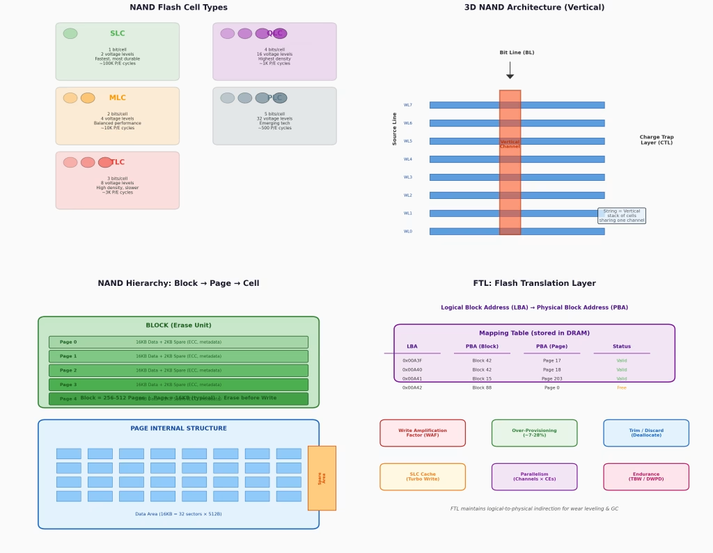
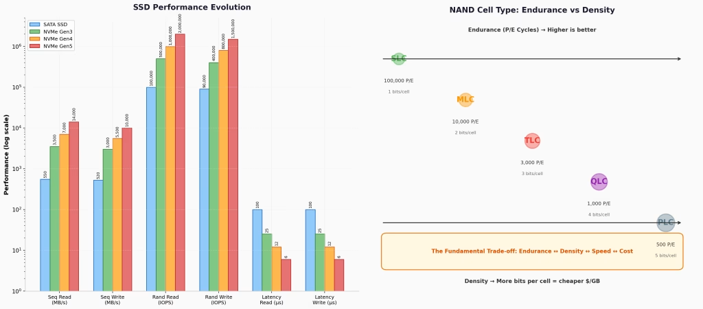
- SLC (Single-Level Cell): 1 bit per cell, 2 voltage levels, ~100K P/E cycles, fastest
- MLC (Multi-Level Cell): 2 bits per cell, 4 voltage levels, ~10K P/E cycles
- TLC (Triple-Level Cell): 3 bits per cell, 8 voltage levels, ~3K P/E cycles, most common in consumer SSDs
- QLC (Quad-Level Cell): 4 bits per cell, 16 voltage levels, ~1K P/E cycles, highest density
- PLC (Penta-Level Cell): 5 bits per cell, 32 voltage levels, emerging technology
3D NAND Architecture:
Modern NAND is built vertically rather than horizontally. In 3D NAND (V-NAND, BiCS, CuA), cells are stacked in vertical strings of 96 to 200+ layers. Word Lines (WLs) run horizontally, while vertical channels connect cells in a string. This architecture dramatically increases density without shrinking cell size, improving reliability and reducing cost per gigabyte.
1.5 Power & Protection Components
- Power Loss Protection (PLP): Enterprise SSDs use supercapacitors or tantalum capacitors to provide enough energy during a power failure to flush DRAM caches and mapping tables to NAND.
- Voltage Regulators: Convert host 3.3V/12V to the multiple voltages required by NAND (1.8V I/O, 3.3V core, charge pump voltages up to 20V for programming).
- Temperature Sensors: Monitor die temperature to trigger thermal throttling and prevent NAND damage.
Part 2: NAND Flash Hierarchy & FTL Details
2.1 NAND Hierarchy
NAND flash is organized hierarchically to maximize parallelism:
- Channel: Independent data path from controller to NAND. Modern SSDs have 4-8 channels.
- CE (Chip Enable): Selects a specific die on a channel. Multiple dies share a channel via time-multiplexing.
- Die: A single NAND chip containing planes, blocks, and pages.
- Plane: A die is divided into 2-4 planes that can operate independently or in parallel.
- Block: Contains 256-512 pages. The smallest unit that can be erased.
- Page: Contains 16KB of user data + ~2KB spare area. The smallest unit for read and program operations.
2.2 The Flash Translation Layer (FTL)
The FTL is what makes NAND flash usable as a block device. Without it, the host would need to understand that blocks must be erased before written, that pages cannot be overwritten, and that blocks wear out.
Key FTL Functions:
Address Translation: The FTL maintains a mapping table (L2P: Logical to Physical). When the host writes to LBA 0x00A3F, the FTL allocates a free physical page—say Block 42, Page 17—and records this mapping. On subsequent reads, the FTL looks up LBA 0x00A3F and retrieves data from Block 42, Page 17.
Write Amplification Factor (WAF): Because NAND requires erase-before-write and GC moves valid data, the actual NAND writes exceed host writes. WAF = NAND writes / Host writes. A WAF of 1.0 is ideal; values of 2-4 are common under heavy random write workloads.
Over-Provisioning: SSDs reserve 7-28% of raw NAND capacity as spare area. This hidden space provides:
- Replacement blocks for bad block management
- Buffer space for garbage collection
- Room for wear leveling
SLC Cache: Many TLC/QLC SSDs use a portion of their NAND in SLC mode (1 bit per cell) as a write cache. This provides sustained write speeds until the cache fills, after which writes drop to native TLC/QLC speeds.
TRIM/Discard: When the OS deletes a file, it sends a TRIM command to inform the SSD which LBAs are no longer valid. The FTL can then mark corresponding physical pages as invalid, making GC more efficient.
Part 3: The Complete I/O Lifecycle
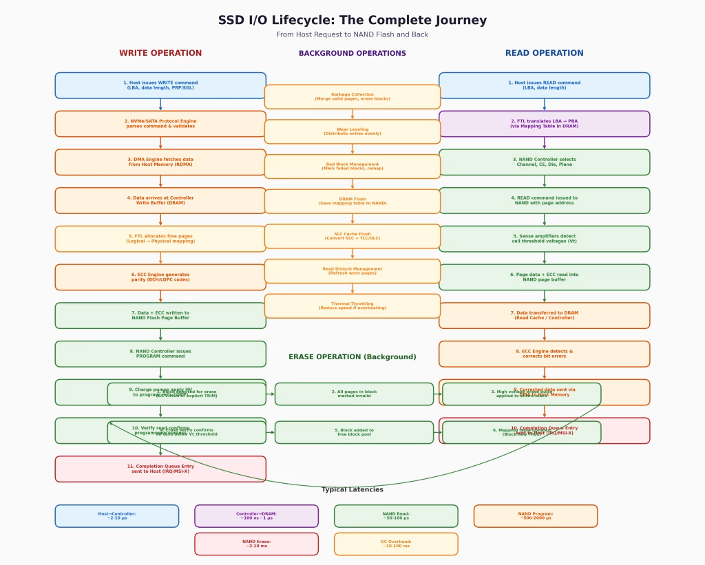
3.1 Write Operation Lifecycle
Step 1: Host Issues Write Command
The host CPU writes a command to the NVMe Submission Queue (SQ) in host memory. The command specifies the starting LBA, data length, and PRP/SGL entries pointing to the data buffer.
Step 2: Doorbell & Command Fetch
The host rings the Tail Doorbell register. The SSD’s DMA engine fetches the command from host memory.
Step 3: Protocol Validation
The NVMe protocol engine validates the command, checks permissions, and ensures the namespace is ready.
Step 4: Data Transfer
The DMA engine fetches write data from host RAM across the PCIe bus into the SSD’s DRAM write buffer.
Step 5: FTL Address Translation
The FTL looks up the LBA in the mapping table. If this LBA was previously written, the old physical page is marked invalid. The FTL allocates a new free physical page from the pool.
Step 6: ECC Generation
The ECC engine computes parity bits for the data. For LDPC, this involves complex iterative encoding algorithms.
Step 7: NAND Programming
The data + ECC + metadata is transferred from DRAM to the NAND die’s page buffer. The NAND controller issues the PROGRAM command with the physical address (channel, CE, die, plane, block, page).
Step 8: Cell Programming
Charge pumps inside the NAND die generate high voltages (15-20V). Using Incremental Step Pulse Programming (ISPP), the controller applies precise voltage pulses to trap electrons in the floating gate or charge trap layer, adjusting the cell’s threshold voltage (Vt) to represent the desired bit pattern.
Step 9: Program Verify
The NAND performs a verify read to confirm cells reached their target Vt levels. If not, additional program pulses are applied.
Step 10: Completion
The SSD writes a Completion Queue Entry (CQE) to the Completion Queue in host memory and optionally triggers an interrupt (MSI-X) to notify the host.
3.2 Read Operation Lifecycle
Step 1: Host Issues Read Command
Similar to write, the host places a READ command in the Submission Queue.
Step 2: FTL Translation
The FTL looks up the LBA in the mapping table to find the physical page address. This DRAM lookup takes ~100 nanoseconds.
Step 3: NAND Selection
The NAND controller selects the appropriate channel, CE, die, and plane based on the PBA.
Step 4: NAND Read Command
The controller sends the READ command with the page address to the NAND die.
Step 5: Sense Amplification
Inside the NAND die, sense amplifiers apply reference voltages to determine each cell’s threshold voltage. This is the slowest step (~50-100 μs) because the bit lines must settle.
Step 6: Page Buffer Transfer
The entire page (16KB + spare) is read into the NAND’s internal page buffer.
Step 7: Data Transfer to DRAM
The page is transferred from NAND to the SSD’s DRAM cache via the ONFI/Toggle DDR interface.
Step 8: ECC Decoding
The ECC engine reads the data and parity bits. If bit errors are detected (common in TLC/QLC), the LDPC decoder iteratively corrects them. If errors exceed correction capability, the drive may use RAID-like recovery across dies or report an uncorrectable error.
Step 9: Data to Host
The DMA engine transfers corrected data from DRAM to the host memory buffer specified in the original command.
Step 10: Completion
A CQE is posted, and the host is notified.
3.3 Erase Operation
NAND flash cannot overwrite data in-place. Erasure must occur at the block level:
- Selection: GC or explicit TRIM identifies a block for erasure.
- Invalidation: All pages in the block are marked invalid in the FTL metadata.
- Erase Pulse: The NAND applies a high-voltage erase pulse to the entire block, pulling electrons out of the floating gates.
- Erase Verify: The block is verified to ensure all cells are below the erased threshold voltage.
- Free Pool: The block is added back to the free block pool.
- Mapping Update: The FTL records the block as free.
Erase latency is the slowest NAND operation at ~2-10 ms.
Part 4: Background Operations
SSDs perform critical maintenance work invisible to the host:
Garbage Collection (GC): When free space runs low, the SSD identifies blocks with the most invalid pages, copies remaining valid pages to new blocks, and erases the old blocks. GC is the primary source of performance inconsistency and write amplification.
Wear Leveling: Static wear leveling moves cold (infrequently changed) data to blocks with high erase counts, while dynamic wear leveling distributes new writes evenly.
Read Disturb Management: Reading a page thousands of times can subtly alter neighboring pages’ charge states. The SSD tracks read counts and refreshes at-risk pages.
Thermal Throttling: If the controller or NAND exceeds safe temperatures (typically 70-85°C), the SSD reduces clock speeds and parallelism to prevent damage.
DRAM Flush: Periodically, the FTL writes the mapping table and metadata from DRAM to NAND to ensure recoverability after power loss.
SLC Cache Flush: For drives with pseudo-SLC caches, background processes convert SLC-written data to TLC/QLC format to free up fast SLC space.
Part 5: Performance Characteristics
5.1 Interface Evolution
| Generation | Seq Read | Seq Write | Rand Read IOPS | Rand Write IOPS | Read Latency |
|---|---|---|---|---|---|
| SATA SSD | ~550 MB/s | ~520 MB/s | ~100K | ~90K | ~100 μs |
| NVMe Gen3 | ~3,500 MB/s | ~3,000 MB/s | ~500K | ~400K | ~25 μs |
| NVMe Gen4 | ~7,000 MB/s | ~5,500 MB/s | ~1M | ~800K | ~12 μs |
| NVMe Gen5 | ~14,000 MB/s | ~10,000 MB/s | ~2M | ~1.5M | ~6 μs |
5.2 The Endurance-Density Trade-off
There is no free lunch in NAND flash. As we store more bits per cell:
- Density increases → Lower cost per GB
- Endurance decreases → Fewer program/erase cycles before failure
- Speed decreases → More voltage levels require finer discrimination and slower programming
- Power increases → More complex programming algorithms
Enterprise SSDs often use eTLC (enterprise TLC) with better validation and over-provisioning, while consumer drives push QLC to maximize capacity at minimal cost.
Part 6: Key Metrics and Specifications
TBW (Terabytes Written): Total bytes the SSD is rated to write before failure. A 1TB drive with 600 TBW can sustain ~0.3 full drive writes per day (DWPD) over 5 years.
DWPD (Drive Writes Per Day): Enterprise metric indicating how many times the entire drive capacity can be written daily throughout the warranty period.
MTBF (Mean Time Between Failures): Typically 1.5-2 million hours for enterprise SSDs.
UBER (Uncorrectable Bit Error Rate): The probability of an uncorrectable error, typically <1 sector per 10^17 bits read for enterprise drives.
Conclusion
An SSD is one of the most sophisticated embedded systems in modern computing. What appears to the host as a simple block device is actually a parallel computer managing thousands of NAND dies, executing complex error-correction algorithms, performing real-time garbage collection, and maintaining massive translation tables—all while delivering microsecond-level latencies and millions of IOPS.
Understanding this architecture is essential for system designers, storage administrators, and developers who want to optimize application performance, predict drive longevity, or troubleshoot anomalous behavior. The next time you save a file and marvel at the speed, remember: behind that simple write operation is an intricate dance of charge pumps, LDPC decoders, wear-leveling algorithms, and mapping tables working in perfect harmony.
